Piezoresponse Force Microscopy (PFM)
Why use PFM?
Ferroelectric materials are used in a wide range of technologies, from non-volatile memories and sensors to actuators and energy-harvesting devices. Their functionality arises from the arrangement and switching of ferroelectric domains regions where the electric polarization points in different directions. Understanding how these domains form, evolve and respond to external stimuli is essential for improving device performance.
Piezoresponse Force Microscopy (PFM) is one of the most powerful techniques for studying ferroelectric materials at the nanoscale. Since its introduction more than three decades ago, PFM has evolved from a simple domain imaging method into a versatile characterization tool capable of imaging, manipulating and measuring local electromechanical behaviour with nanometre-scale resolution. Today, it is considered one of the cornerstone techniques in nanoferroic research.
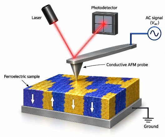
Unlike conventional electrical measurements, which provide only an average response over an entire sample, PFM reveals the behaviour of individual domains and domain walls, allowing researchers to investigate local switching processes that govern the macroscopic properties of ferroelectric materials.
In addition to imaging, AFM is capable of measuring the forces of interaction between the AFM tip and the surface. The high sensitivity of FM-AFM allows us to measure forces as low as a few piconewtons. At the moment, this is not possible with any commercially available AFMs and the force sensitivity is comparable with optical tweezers.
How does PFM work?
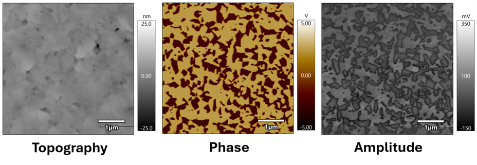
PFM measures the nanoscale surface deformation induced by an applied alternating current (AC) bias, enabling nanoscale mapping of electromechanical response and, under appropriate experimental conditions, the investigation of domain orientation and polarization switching. During a measurement, a conductive AFM tip is brought into contact with the sample surface while a small AC voltage is applied to the tip. Owing to the converse piezoelectric effect, ferroelectric materials undergo periodic surface deformation in response to the applied electric field. These tiny surface deformations deflect the AFM cantilever, whose motion is detected by the AFM laser system. The measured response consists of two complementary PFM signals (Amplitude and Phase; detected using Lock-in technique) along with the topographic mapping. Amplitude indicates the magnitude of the local electromechanical response. Phase indicates the sign of the electromechanical response relative to the applied voltage and, for simple 180° domains under appropriate measurement conditions, can distinguish opposite polarization orientations. This allows researchers to quantify local piezoelectric response under idealized conditions, visualize polarization switching, and analyse hysteresis behaviour at the nanoscale.
What can PFM measure?
One of the greatest strengths of PFM is that it combines imaging, electrical manipulation and local property measurements within a single experiment.
High-resolution domain imaging: PFM maps local electromechanical contrast associated with ferroelectric domains. This enables researchers to study domain configurations, domain-wall structures and polarization patterns that cannot be resolved using conventional electrical measurements. Because the electric field is confined beneath the nanoscale tip, PFM can image ferroelectric domains with spatial resolutions well below 100 nm.
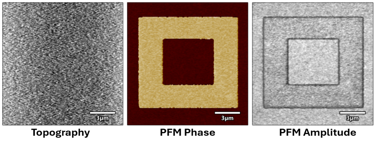
Domain switching: By applying voltage above coercive field, the AFM tip can locally reverse the polarization. This allows domains to be written, erased and rewritten with nanometre precision while simultaneously monitoring the switching dynamics.
Local electromechanical properties: PFM can also measure local switching characteristics, including coercive voltage, nucleation behaviour, piezoelectric response and hysteresis loops. These measurements provide valuable insight into how microstructure influences ferroelectric performance.
PFM modes
Advances in ferroelectric research have driven the development of specialized PFM techniques, enabling comprehensive investigation of these materials at the nanoscale.
Single-Frequency PFM (SF-PFM)
In this conventional mode, the cantilever is excited using a single AC frequency while the amplitude and phase of the electromechanical response are measured. Off-resonance PFM: Operates below the contact resonance, providing a more quantitative piezoresponse but with lower signal sensitivity. On-resonance PFM: Operates near the contact resonance,enhancing signal sensitivity, but also increasing sensitivity to variations in contact stiffness, resonance frequency and local mechanical properties.
Dual AC Resonance Tracking (DART-PFM)
DART is an advanced resonance-tracking method developed to reduce artefacts associated with shifts in the contact resonance during PFM imaging. It continuously tracks the cantilever contact resonance using two closely spaced AC excitation frequencies. By maintaining excitation close to the contact resonance during scanning, DART improves sensitivity and reduces variations caused by resonance-frequency shifts, although interpretation may still be affected by contact mechanics and abrupt changes in surface properties.
Band Excitation PFM Spectroscopy (BEPS)
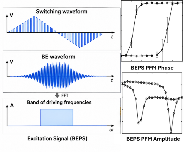
Band Excitation PFM excites the cantilever over a defined frequency band and records the contact-resonance spectrum at each measurement point. Fitting the spectrum provides the response amplitude, phase, resonance frequency and quality factor. In Band Excitation PFM Spectroscopy, this frequency-band measurement is repeated during a DC-bias waveform, allowing local switching behaviour and changes in contact resonance to be examined simultaneously.
Vector PFM
Vector PFM combines vertical and lateral measurements to probe out-of-plane and in-plane electromechanical components. Because lateral PFM is sensitive primarily to the component perpendicular to the cantilever axis, reconstruction of the full polarization vector generally requires measurements at multiple sample or cantilever orientations.
Switching Spectroscopy PFM (SS-PFM)
Switching Spectroscopy PFM extends conventional imaging by recording a local electromechanical hysteresis loop at each measurement point. Spatial maps of switching parameters, including coercive voltage, nucleation bias and imprint can then be generated, providing insight into how local microstructure influences polarization switching across the sample.
Ferroelectric Domain Lithography
PFM can also be used as a nanoscale lithography tool to precisely engineer ferroelectric domain structures. By applying a controlled bias through the conductive AFM tip, the local polarization can be selectively switched to create predefined patterns on ferroelectric surfaces. Common demonstrations include box-in-box poling, where alternating square regions are written with opposite polarization orientations to verify local switching and domain stability. More complex patterns, such as QR codes or artistic bitmap images, can also be created using AFM tip bias lithography. In the example shown, a QR code bitmap is written onto a hafnia thin film using AFM tip bias lithography. Subsequent PFM imaging clearly resolves the written domain pattern, demonstrating the potential of domain engineering for high-density data storage, reconfigurable electronic devices, and nanoscale patterning.

Challenges of PFM
Although PFM is a powerful nanoscale characterization technique, interpreting its results requires careful consideration. The measured electromechanical response is not always produced solely by the converse piezoelectric effect. Electrostatic interactions, electrostriction, charge injection, ionic migration, electrochemical strain, and environmental factors such as humidity can all contribute to the measured signal, sometimes producing responses that resemble ferroelectric switching in materials that are not genuinely ferroelectric. In addition, PFM measurements are influenced by tip-sample contact mechanics. Variations in contact stiffness, surface roughness, and resonance frequency can introduce topographic cross-talk and affect the measured amplitude and phase response. For these reasons, PFM should not be regarded as a standalone proof of ferroelectricity. Reliable interpretation requires careful experimental design, appropriate control measurements, and complementary characterization techniques to confirm the origin of the observed electromechanical response.
Applications of PFM
Over the past three decades, PFM has transformed our understanding of ferroelectric and functional materials by enabling researchers to image, manipulate, and quantify nanoscale electromechanical behaviour under idealized conditions. Beyond conventional domain imaging, PFM has played a key role in discovering new physical phenomena and exploring next-generation electronic devices. Today, PFM is widely used to investigate:
Domain-wall dynamics and domain engineering: studying domain nucleation, growth, motion, pinning, and switching mechanisms.
Local hysteresis and switching spectroscopy: measuring nanoscale polarization switching, coercive voltage, imprint, and electromechanical response.
Relaxor ferroelectrics: investigating polar nanoregions and spatially heterogeneous electromechanical behaviour.
2D and van der Waals materials: probing ferroelectricity and polarization switching in ultrathin and layered materials.
Flexoelectricity: studying polarization generated by strain gradients, particularly at the nanoscale.
Electrochemical and ionic materials: probing electrically driven ionic motion and electrochemical strain, although these responses need careful separation from genuine piezoelectric/ferroelectric signals.
Energy-harvesting materials: characterizing local piezoelectric behaviour in materials intended for mechanical-to-electrical energy conversion.
Biomaterials and biological systems: mapping nanoscale electromechanical and piezoelectric responses in biological materials such as collagen, bone, teeth, tendon, cartilage, proteins, and other biological tissues, extending PFM beyond conventional inorganic ferroelectrics.
Phase transitions: mapping changes in polarization and electromechanical response across temperature-, electric-field-, or stress-driven transitions.
Defects and interfaces: examining how grain boundaries, vacancies, interfaces, and other defects affect local polarization and switching.
Data-storage and neuromorphic devices: studying nanoscale switching relevant to non-volatile memories, memristors, and synaptic-device concepts.
These applications have established PFM as one of the most versatile nanoscale characterization techniques in modern materials science, bridging fundamental research with the development of future memory, sensing, energy, and nanoelectronic technologies.
Summary
PFM provides unparalleled insight into the nanoscale behaviour of ferroelectric materials by combining domain imaging, polarization switching, and local electromechanical characterization in a single technique. Its versatility and high spatial resolution make it an essential tool for both fundamental research and advanced device development.
Quisque iaculis facilisis lacinia. Mauris euismod pellentesque tellus sit amet mollis.