Feeling the Invisible: A Hands-On Journey into Nanoscience and AFM

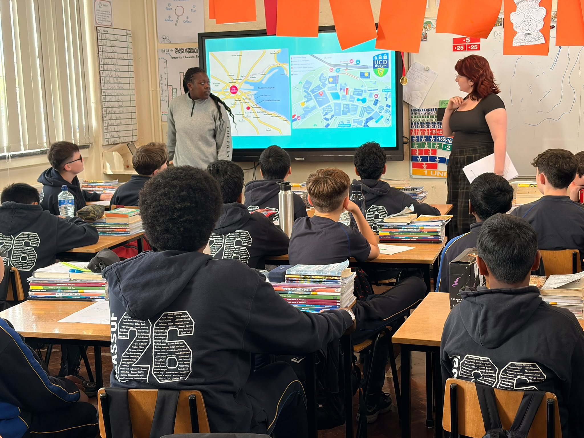
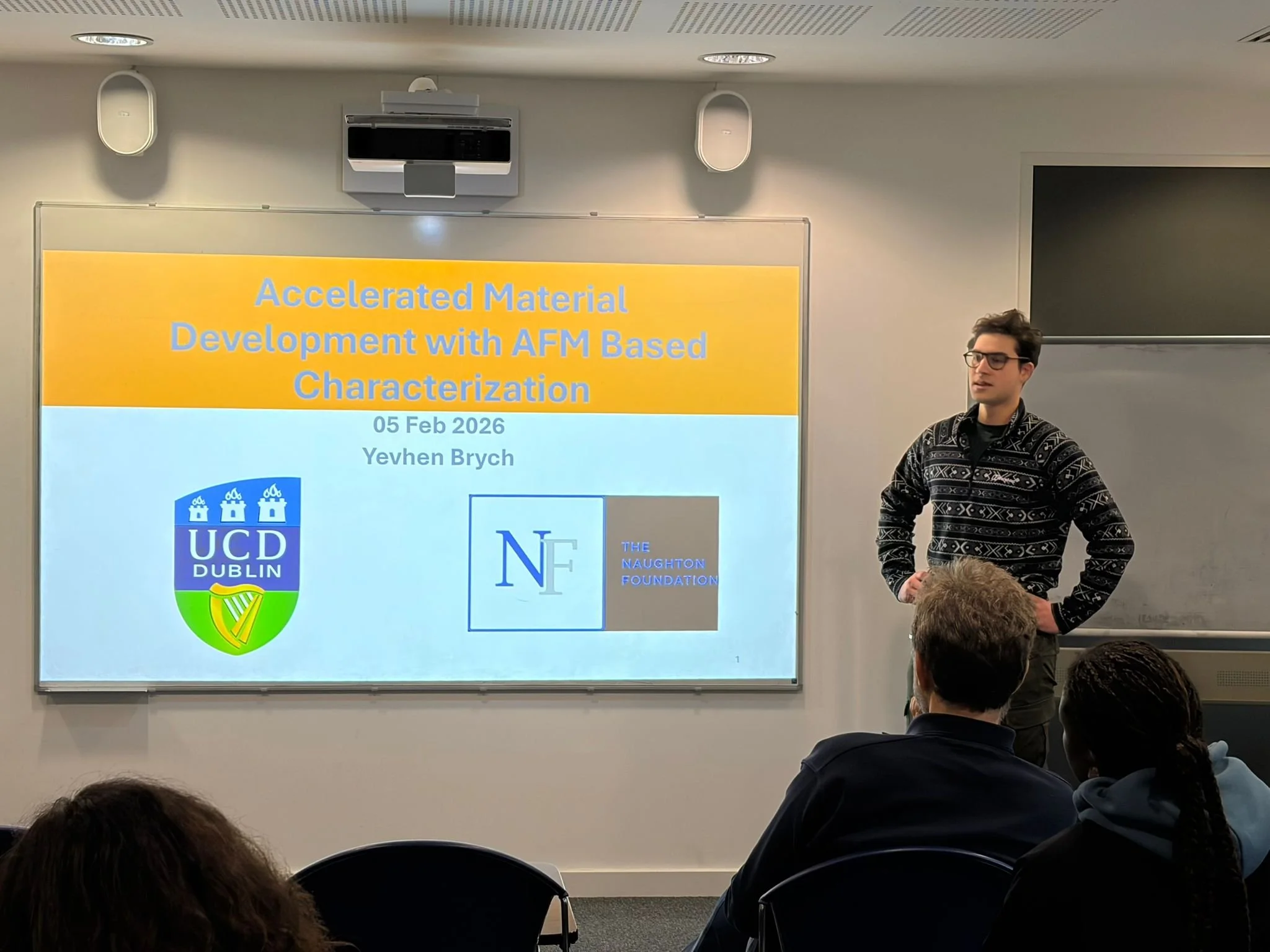
On May 18th, members of the Nanoscale Function Group had the pleasure of visiting Drimnagh Castle Boys Primary School to deliver an outreach session. We introduced the 6th class students to the  world of nanoscience and the Atomic Force Microscope 

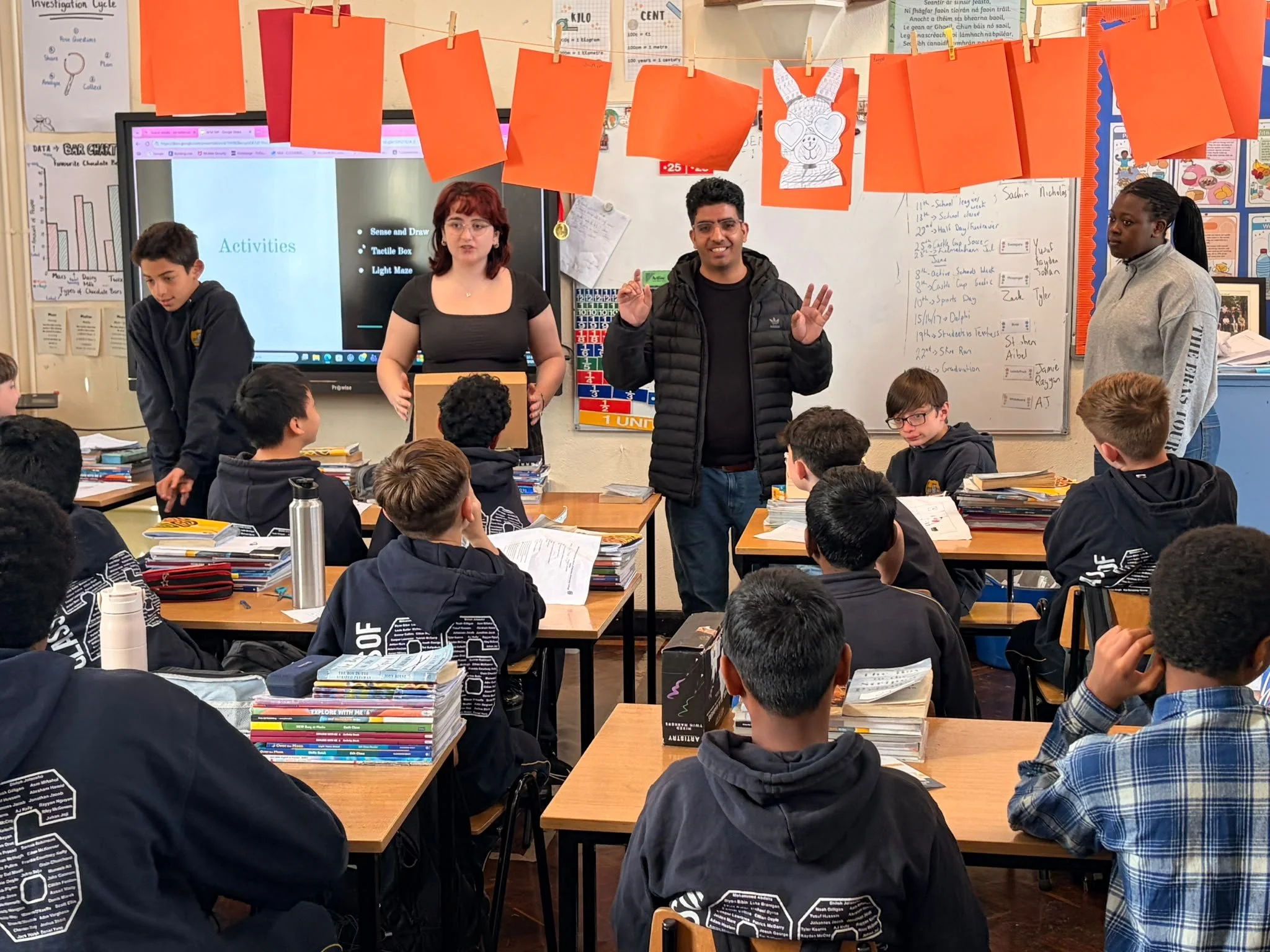
The session aimed to spark curiosity and show students that science is not only exciting but that it's accessible and that it connects them to the world. We began by exploring STEM and STEAM concepts, discussing how science, technology, engineering, arts, and mathematics influence everyday life. Students were encouraged to think about the technology and innovation surrounding them and to challenge common stereotypes about who can become a scientist students.  

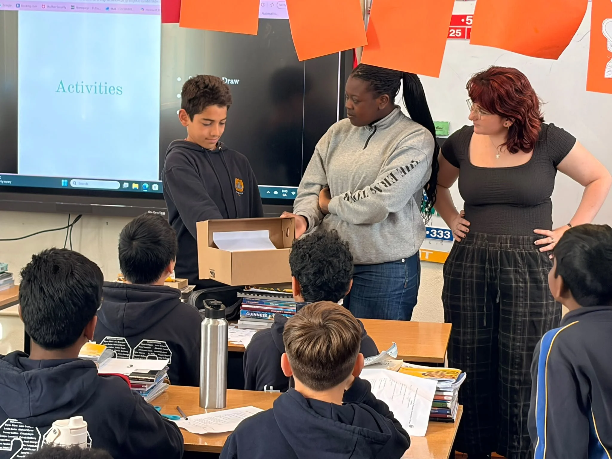
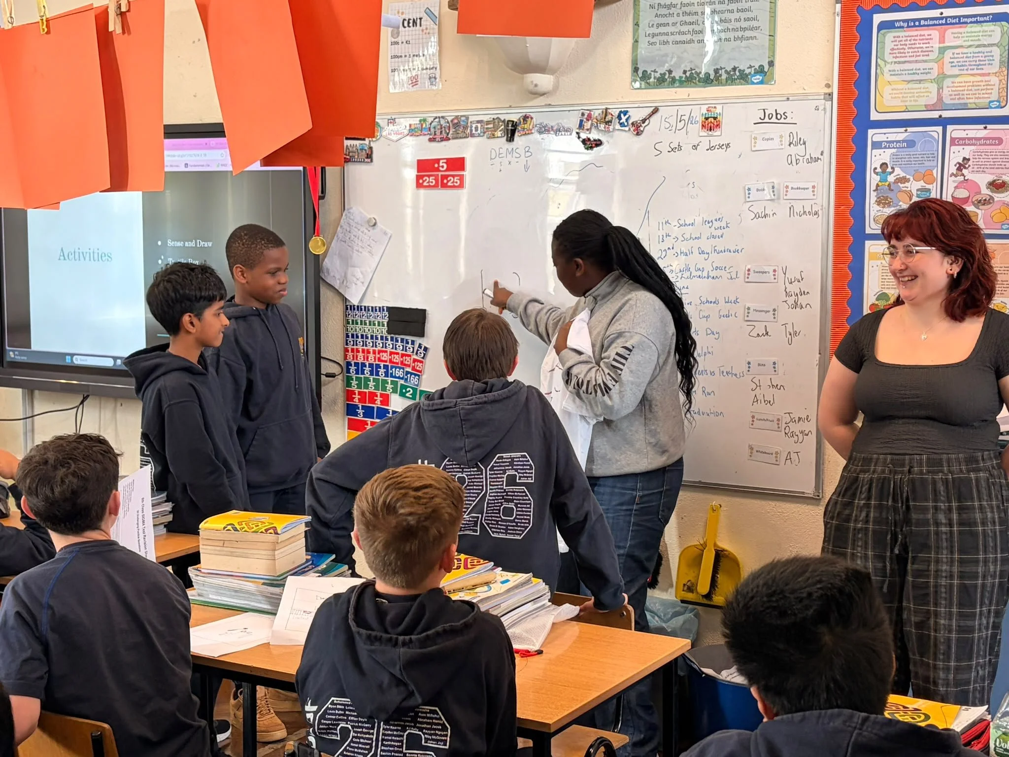
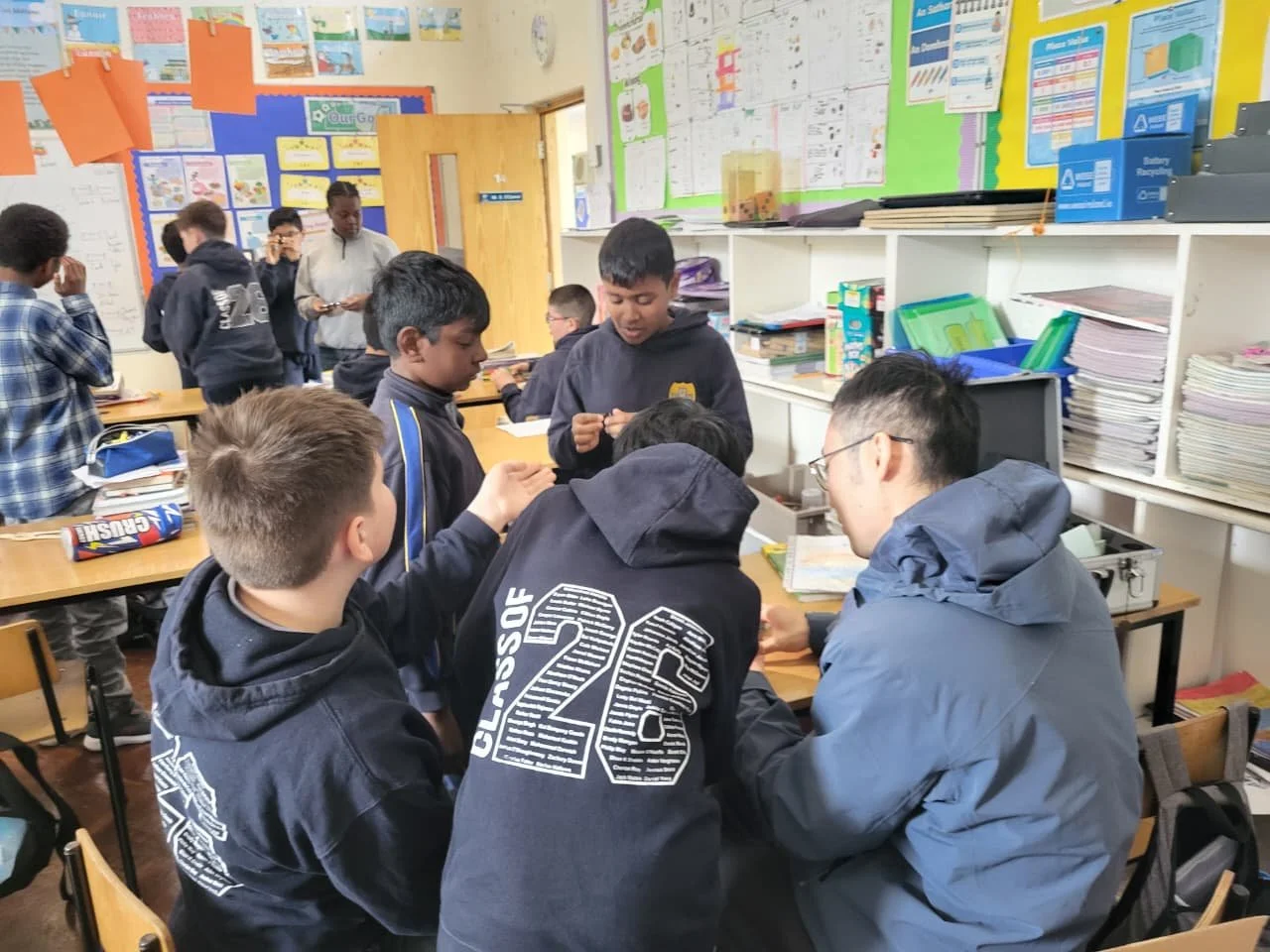
We discussed the work done in the Nanoscale function group and introduced the students to the Atomic Force Microscope. Instead of relying on sight alone, students learned how an AFM can "feel" surfaces using an ultra-sharp tip, similar to reading braille at the nanoscale. Through interactive explanations and demonstrations, we explored how scientists can investigate structures at an atomic scale. To bring these ideas to life, students participated in several hands-on activities designed around the concept of touch and sensing. Through tactile games and challenges, they experienced how information can be gathered without relying on vision alone, mirroring the principles used in Atomic Force Microscopy.

The session also highlighted how AFM research contributes to important areas such as healthcare, renewable energy, materials science, batteries, and food technology, giving students a glimpse into how research at the nanoscale can impact society.

We would like to thank the students and staff at Drimnagh Castle Boys Primary School for their enthusiasm, engagement, and warm welcome. It was a fantastic opportunity to share our research and encourage the next generation of scientists to ask questions, stay curious, and discover that science can be for everyone. The Nanoscale Function Group looks forward to continuing its outreach efforts and creating meaningful opportunities that make science engaging, inclusive, and inspiring for future generations.


E-MRS Spring Meeting 2026 in Strasbourg, France

Waseem Ahmad Wani represented the NFG group at the E-MRS Spring Meeting 2026 (with 2300 participants) in Strasbourg, France, where he delivered two oral presentations highlighting recent advances in hafnia-based ferroelectric materials. In his first presentation, “Probing Domain Stability in Hafnia Thin Films,” Waseem discussed the factors governing ferroelectric domain switching and retention at the nanoscale. The study provided new insights into role of environmental control. probe-surface interactions, charge screening effects, and the reliable characterization of ferroelectric hafnia using piezoresponse force microscopy.

His second talk, “Nanoscale Ferroelectric Response in Plasma-Processed HZO,” focused on how plasma-assisted processing influences ferroelectric phase formation and domain stability in hafnium zirconium oxide (HZO) thin films. The work highlighted the crucial roles of processing conditions, electrodes, and mechanical and electrical control in optimizing ferroelectric performance.

The conference provided an excellent opportunity to share our latest research, engage with the international materials science community, and explore emerging developments in ferroelectrics and functional oxide materials. Great science, inspiring discussions, new friends, new collaborations, and wonderful memories along the way.

#EMRS2026 #Hafnia #Ferroelectrics #MaterialsScience #UCD

Catching up on the latest in nano-machining?

Last Friday, Nawal presented her research at the UCD–TUD International Day of Light, hosted at the TU Dublin.
She shared insights into how Atomic Force Microscopy (AFM) can be utilized to machine hard and brittle crystals at the nanoscale. Crucially, Nawal discussed how nanomachining can complement existing nanofabrication techniques—and how combining these methods could fundamentally shape the future of Nanophotonics.

NFG Outreach Showcase

We are delighted to share that the outreach work of the Nanoscale Function Group was highlighted at the first Widening Participation Outreach Good Practice Showcase Event, held on May 7th, 2026, at the Access & Lifelong Learning Centre in University College Dublin.

It was a privileged moment for us to see our outreach initiatives recognised alongside the fantastic work being carried out across the different schools and groups within UCD. The event celebrated efforts to widen participation in science and higher education, while encouraging engagement with students from diverse backgrounds.

A special thank you to Niamh O Sullivan for shining a light on the outreach activities organised by members of the Nanoscale Function Group. We are excited to continue creating opportunities that inspire curiosity, inclusion, and the next generation of scientists. We look forward to continuing our outreach efforts and inspiring the next generation of scientists through meaningful and inclusive engagement activities. (Michelle & Waseem)

Celebrating a Milestone in Nawal’s Journey

On 30th March 2026, Nawal was awarded with the Outstanding Student Award by the UCD College of Science.

Presented during a special ceremony celebrating women in science, this recognition highlights her dedication, hard work, and academic excellence. Being acknowledged in an environment that supports and uplifts women in research makes this achievement even more meaningful.

This moment marks not just a milestone, but a reflection of Nawal’s passion and perseverance throughout her journey.

Congratulations to Nawal on this well-deserved recognition. We wish her continued success and look forward to celebrating many more achievements in the future.

Congratulations to Nawal on Successfully Passing Her PhD Stage Transfer Assessment

On February 6th, 2026, Nawal successfully progressed to Stage 2 of her PhD studies.

Nawal’s work focuses on lithium niobate, the “industry standard” for optical modulators. While this material is already a cornerstone of modern optics, Nawal is looking to push its boundaries by miniaturizing components to the chip scale. This has the potential to transform a wide-range of electro-optic applications, from ultra-sensitive sensing to advanced catalysis.

Nawal’s stage transfer presentation centered on Atomic Force Microscopy (AFM)-based nanolithography. By optimizing machining techniques, she is discovering how to sculpt lithium niobate with high precision.

As she enters this next stage of her PhD, she is looking further into integrating the technique with ferroelectric domain inversion. These developments will advance the next generation of lithium niobate based on-chip scale devices.

From Probing Surfaces to Probing Success: Yevhen Passes His Stage Transfer Assessment

By successfully passing his Stage Transfer Assessment (STA), Yevhen has reached an important milestone in his PhD journey, officially transitioning from a probationary research student to a fully registered PhD candidate. In an engaging talk, he shared his research on using Atomic Force Microscopy (AFM) to study advanced semiconductor materials at the nanoscale. His presentation also demonstrated insightful research plans and a strong foundation for exciting results ahead.

In his presentation, Yevhen highlighted an interesting idea: defects in materials, often seen as imperfections, can give rise to some of their most useful properties. From controlling conductivity to enabling quantum functionalities, these tiny irregularities can have a surprisingly large impact on device performance.

Yevhen’s project focuses on probing such defects and dopants inside materials and devices, aiming to understand their diverse electrical behaviour at the nanoscale. To achieve this, he uses advanced AFM techniques including Electrostatic Force Microscopy (EFM), Conductive-AFM, and Kelvin Probe Force Microscopy (KPFM), which allow researchers to map electrical properties with extremely high spatial resolution.

Looking ahead, Yevhen plans to expand this work using Scanning Microwave Impedance Microscopy (sMIM) and apply these techniques to doped silicon carbide samples from collaborators, potentially opening new insights into materials relevant for quantum technologies.

In many ways, Yevhen’s research is about thinking small to make a big impact, probing materials at the nanoscale to enable the next generation of powerful electronic devices.

Congratulations again to Yevhen on this milestone. We look forward to seeing the exciting results that will come from his work!

DREAM-Nano Final Conference

On 21 November 2025, our group hosted the final conference of DREAM-Nano, a Una Europa seed-funded initiative focused on designing responsive nanomaterials for nanomedicine. The event opened with a guided tour of UCD Conway Institute, where participants visited the metabolomics, proteomics, flow cytometry, and imaging core facilities. This tour highlighted the advanced infrastructure that supports collaborative biomedical research at UCD.

Topics of talks ranged from magnetic nanoparticles for cancer therapy and imaging, to wearable biosensors, plasmonic DNA diagnostics, and biodegradable platforms for gene delivery. In the closing session, Maryia Rohava from UCD Research presented upcoming funding opportunities under Horizon Europe.

With contributions from universities and biotechnology companies, the DREAM-Nano project successfully created a foundation for long-term international collaboration in nanomedicine.

Breaking Voltage Limits: Measuring Over 400 V with Dual Harmonic KPFM

At the IEEE ISAF-ICE-ISIF-PFM 2025 conference, held July 13–18, 2025, in Graz, Austria, Dr. Qiancheng Zhang presented a breakthrough in high surface potential measurement — Dual Harmonic Kelvin Probe Force Microscopy (DH-KPFM) now capable of measuring surface potentials exceeding 400 volts.

Traditional KPFM techniques, while powerful, typically max out at 10 V and rely on a feedback loop. Dr. Zhang’s work pushes these boundaries by using DH-KPFM—an open-loop, AC-only method that eliminates the need for DC bias and enables measurements in liquid environments or on DC-sensitive materials.

The stiffer cantilevers dramatically increase the max measurable voltage range, with a 247 N/m cantilever successfully detecting up to 432.9 V. This high-voltage capability was further applied to measure pyroelectric coefficients of materials like lithium niobate and TGS.

This advancement opens new doors for nanoscale measurements in high-field materials and extreme conditions. We're now seeking collaborations where high-voltage, liquid-phase, or DC-sensitive surface potential measurements are needed.