AFM nanomachining
What is AFM nanomachining?
AFM nanomachining is a contact mode, mechanical material removal process with nanoscale precision. A sharp probe, typically a diamond-coated silicon tip or a single crystal diamond tip for hard substrates, is mounted on a microfabricated cantilever. The cantilever is pressed against the surface with a controlled normal force, typically in the range of a few to several hundred micronewtons. Material is displaced or removed by the combined action of indentation and lateral shear, producing grooves, trenches or complex patterns with feature width that can reach well below 100 nm.
Why AFM nanomachining?
Unlike photolithography or electron-beam lithography, AFM nanomachining requires no masks, no resists, and no chemical development steps. It is a direct-write technique that operates entirely in the mechanical domain, making it uniquely suited for prototyping.
How does the technique work?
In contact-mode AFM, cantilever deflection is commonly measured using the optical beam-deflection method, where a laser reflected from the back of the cantilever is detected by a position-sensitive photodetector. As the tip interacts with the surface, the cantilever deflects, shifting the laser spot on the detector. In constant-force operation, a feedback loop maintains a fixed deflection setpoint, keeping the applied force constant while the tip rasters across the surface.
For nanomachining, the setpoint force is deliberately increased far beyond the imaging threshold. The tip is now pressed into the surface hard enough to induce plastic deformation, the material beneath the tip cannot elastically recover, and a groove is left behind. The depth and width of that groove depend on several interlinked factors including normal force, scan speed, number of passes, and tip geometry.
Two principal machining modes are used in practice. In scratch (vector) machining, the tip follows a defined path, a line, curve, or arbitrary vector, to cut individual groves or gratings. In area (raster) machining, the tip sweeps over a rectangular region pass-by-pass, machining the entire area to a target depth and producing flat-bottom trenches or stepped platforms.
One practical advantage of AFM nanomachining is that the same instrument can be used for both fabrication and characterisation. There is no need to transfer the sample to a separate metrology tool between fabrication and inspection, the AFM can image surfaces before, during (between passes), and after machining, making fabrication straightforward.
Applications
Ferroelectric nanostructures (BiFeO3): Rodriguez and colleagues demonstrated that AFM-based mechanical nanomachining can directly pattern BiFeO3 thin films, a multiferroic material combining ferroelectricity and antiferromagnetism1. Fig. 1 shows an AFM machined harp on BiFeO3 thin film.
3D Tomographic Imaging of Ferroelectrics: Tomographic AFM uses nanomachining to sequentially remove thin layers of a ferroelectric and image the exposed surface after each pass. This produces a volumetric map of the ferroelectric domain structure over a controlled depth. This application repurposes the machining process as a subsurface characterisation tool, revealing domain configurations that no surface-only technique can access. Recent work by Sharma et al. has extended this approach to hexagonal manganite single-crystals, mapping the three-dimensional morphology and conductivity of domain wall networks buried beneath the sample surface.2 The same layer-removal strategy has also been applied to free-standing ferroelastic thin films, where AFM milling provided precise thickness control for correlative in situ TEM studies of size-dependent domain wall behaviour.3
Silicon and semiconductor patterning: Single-crystal silicon has been patterned extensively with diamond AFM tips, producing groove arrays, step features, and arbitrary 2D patterns with sub-100 nm feature widths. This work established foundational depth-force relationships and tip wear models used across all subsequent AFM nanomachining research on hard substrates.
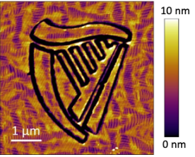
Fig. 1. AFM height image of a machined harp from UCD logo on BiFeO3 thin film
References
F. Zhang et al., “Investigation of AFM-based machining of ferroelectric thin films at the nanoscale” J. Appl. Phys.127,3 (2020)
N. Sharma et al., “AFM-Based Functional Tomography – To Mill or Not to Mill, that is the Question!” Adv. Mater. Interfaces 12, 9 (2025)
B. Scott et al., “Evidence of the Monopolar-Dipolar Crossover Regime: A Multiscale Study of Ferroelastic Domains by In Situ Microscopy Techniques” Small 20, 35 (2024)
Quisque iaculis facilisis lacinia. Mauris euismod pellentesque tellus sit amet mollis.